Servo motors can be used with success in several different robotic applications. The have a very simple electrical interface and are available in a great assortment of specifications and prices.
Usually one can get started with a very cheap one. This paper will show how to control one of these servos using a PC and a microchip PIC microcontroller. For read more see here.
December 23, 2009
Programming Lego robot using NQC
The Lego Minstroms and CyberMaster robots are wonderful new toys from wich a wide variaty of robots can be contructed, that can programed to do all sorts of complicated tasks. Unfortunately, the software that comes with the robots is , although visually attractive, rather limited in functionality. Hence, it can only be used for simple tasks.
To unleash the full power of robots, you need a different programmming environment. NQC is prograamming language written by Dave Baum, that was especially designed for the Lego robots. For complete report can look at here.
To unleash the full power of robots, you need a different programmming environment. NQC is prograamming language written by Dave Baum, that was especially designed for the Lego robots. For complete report can look at here.
December 22, 2009
Microprocessor Controlled Vehicle Robot
The UEL group project should force students working together as a small group. Therefore a vehicle, called "MIcromouse" was to be designed and built up.
Aim of project is to win the final race, wich consist of three round each 2 lap on a small rectangular maze. For the complete report can read on here
Aim of project is to win the final race, wich consist of three round each 2 lap on a small rectangular maze. For the complete report can read on here
December 21, 2009
Making the VFO PLL for High Frequency
Homebrew multiband SSB transceiver part 6
Programmable IC TC 9122 DEVIDER was only able to divide frequency up to approximately 14 MHz at 6-volt voltage.
For the ability devider is 1 to 3999.
Therefore, if the frequency that must be shared exceeds the capacity it should be held down Conversion, which required pre-mixer.
For example the 5266 KHz IF frequency to be work in the 14250 KHz band is required to vfo frequency 14250 + 5266 = 19516 KHz PLL so must be made
who worked around 19516 KHz.
 In this project the set Oscilator Reference 1KHz, was
Xtal oscillator taken 16 MHz. Because 16MHz crystal
available lots in the market.
 From the block diagram above can be calculated that the frequency of
into the TC 9122 to work on 14250KHz is 19516KHz -16000KHz = 3516KHz. 3516 numbers are still under number 3999 of the divider TC 9122. So the 14250KHz working frequency must be programmed for the TC9122 to 3516 that if written in BCD: 11 0101 0001 0110
Control circuit used for IC CD4029 up / down counter that can be programmed.
 To move UP / DOWN is used two IC CD4011 also as debouncer. Encoder dial can
use mechanical systems that available in the market. Dial encoder can be used from the component MOUSE computer unused / damaged.
To make the VFO on the other band, the market can be found in the crystal
with frequency 3, 5, 6, 8, 10 and 16 MHz that can be tried to achieve the desired frequency band
December 18, 2009
System to make VFO PLL (phase lock loop)
Homebrew multiband SSB transceiver part 5
The basis of the PLL circuit system can be described as below:

a. Frequency Reference
This circuit has a stable output so it should be raised through Xtal oscillator, which then split - for to obtain a low frequency such as 1 KHz. So F1 = 1kHz
b. Comparator:
This circuit has 2 input frequency F1 and F2 and have an output DC voltage. The nature of this circuit is: If F1 = F2 then the output is a constant DC voltage. And If F1 is not F2 is equal to the DC output is shaped sawtooth (saw tooth). Output voltage is fed to the VCO circuit.
c. VCO = Voltage Controll Oscilator:
This circuit is a series of Variable frequency oscillator which is controlled by frequencynya output voltage. In this PLL circuit that controls the voltage is voltage output of the Comparator. From the picture above if F1 = F2 = 1 KHz then the voltage output of Comparator constant so that the output frequency of VCO fixed or stable. In such circumstances This system is said in LOCK state.
d. PROGRAMMABLE DEVIDER:
This circuit is a circuit that can divide frequency, has an input and an output. TC9122 IC can be divided from 1 to 3999.
For this programming provided on 14 pin TC9122 for BCD numbers,
A1A2A3A4 B1B2B3B4 C1C2C3C4 D1D2.
If you want to deprogram the 3149 PIN 2 must be in give voltage:
1001 0010 1000 11.
1 = high (no tension) and 0 = low (no voltage)
If N is made 3149's F1 = 1 KHz the system in will LOCK when Fout = 3149 MHz. The formula is
Fout = N = Nx F1
divisor program, F1 = freq.Ref
Make Exciter SSB transceiver.
Homebrew multiband SSB transceiver part 4
In a box if there is a TX and a RX is the box can not be called an Transceiver (TRX). Because of a unit will be called a transceiver when the unit are Tx and RX. and between the TX and RX there some components such as IF amplifier combined, SSB filter, VFO, power supply and others.
In this project for good efficiency RF amplifiers for transmit and to receive also be incorporated. More and more components / units are held together more quickly and easy to assemble.
In this project is put together is:
a. Power Supply
b. If amplifier
c. SSB filter
d. VFO
e. RF amplifier TX / RX
 Note that in this circuit there are many diodes , A few diodes act as switches and the other as DC current bloking.
Homebrew make IF transformer
Homebrew multiband SSB transceiver part 3
 From the results of experiment for frequewncy around 5 MHz (5.2665MHz) L1 = L2 = 30 wrap 5 Koker wrap on the ferrite core diameter of 6 millim, C1 = 100 pf.
IF amplifier includes Low Power Amplifier so that only need a small current, and a parallel load L1C1 as a band pass filter.
We know that the LC parallel a high impedance, while the bipolar transistor has a medium impedance. As such collector can not be connected directly to point A but ketitik B, That be located where the question point B?
There Rule of Thumb is: Called hot-end point A, point C is called the cold-end if the collector higher impedance point B must be closer to point A. And vice versa if the impedance collector more Low point B closer to point C.
We know that the impedance Z = V / I with a large or small impedance depends on the size of collector currents collector. The smaller the current higher impedance.
The amount of L2 that will roll into the amplifier input The next approximately 1 / 6 of the number of coils L2 and must rolled near point C cold-end.
December 16, 2009
Make SSB Filter
Homebrew multiband SSB transceiver part 2
Experience shows that to make a SSB filter This is the most profitable is to configure Lattice Filter. With this configuration seems to be very easy to achieve a flat top on the pass band, and both have a slope of near symetris, so easy to use to filter the USB and LSB. In this project used two types of crystals each with a frequency X1 = X2 = 5.26665 and 5.26865 MHz.
Note that it has 2 crystal 2 KHz difference. LC components in parallel resonant frequency is set to 5.26765 to form near the top flat. Condensator C1 and C2 expected that the band pass filter becomes wider.

In this project C2 = 10 pf and R1 = R2 = 2.2k. LC1 set Resonant in the middle order bandpass peaks Bandpass near average. L Koker wound on ferrite core 6 mm as many as 45 wrap while C1 = 50 pf. There are several terms for this SSB filter,:
a. Band pass as shown symetris called filters, left and right slopes of the same
b. Boundary slope with flat line is notch filter. In image point X1 is X2 notch below being called top notch.
c. If the carrier frequency in the notch below ditepatkan there will be a SSB USB and vice versa if matched carrier frequency of the notch that will there is SSB LSB d. Thus to change from LSB to the USB is denganmengganti carrier frequency without having to replace filter.
This is one advantage of the filter that symetris.
December 13, 2009
Homebrew Multiband SSB Transceiver part 1
For radio amateurs who enjoy making their own equipment Sure hope some time to make homemade multiband transceiver. Here the author deliberately design a display-oriented SSB transceiver with components that are easy to make and with components easily available in the market. The block diagram of multiband transceiver like the following:
 Figure 1 Multiband SSB Transceiver diagram
From the diagram above transceivers today I want to explain important points only gradually and is the key to the design, are:
1. Make a SSB filter
2. Creating IF amplifier transformers
3. Creating Exciter
4. Making the system PLL VFO for each band ( 3.5, 7, 14, 21, 28 MHz).
5. Creating the DDS VFO (Direct Digital Synthesizer)
6. Digital display.
December 10, 2009
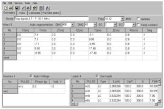
Amateur Radio Antenna Designing Software Use MMANA part 2
Step By Simple Antenna Analysis
During the install, MMANA has prepared many examples of antenna that can be used without need to make a new antenna examples. Various examples can be accessed via the menu MMANA File -> Open, in which there will be some folders containing the antenna examples, such as,
Aperiodic - like Rhombic.
Feeders - feeder antenna.
HF Beam - beam antennas in HF.
HF multiband - multiband antennas in HF.
HF Simple - a simple antenna on HF.
Match - for impedance matching.
Receive - to receiver / radio receiver.
Short - short antenna.
VHF - VHF and UHF antennas.
VHF Beam - antenna beam / yagi in the VHF / UHF. And many more.
If we do not need to tune the antenna to another frequency, then the actual simulation process is very simple.
Several stages / steps that need to be simple to analyze an antenna is as follows,
- Load the file in the desired antenna, through MMANA menu File -> Open -> Folders desired -> Files are in want.
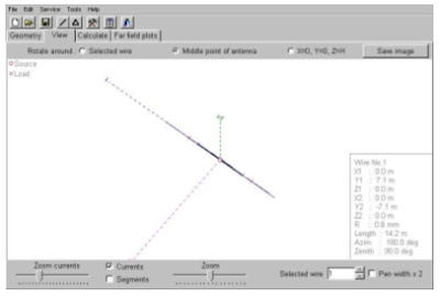
 After the files antenna that we want in the select and the load to MMANA, you will be showing dimensions / geometry of the antenna to be simulated, along with various other information, such as source and load position (coil) of the pairs of antennas.


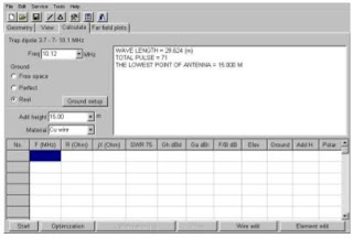
- Click the Calculate menu to prepare to simulate antenna. There are some things we can change in the Calculate menu, namely, operating frequency antenna, tower height, and type antenna material (whether it is a wire or pipe, copper or aluminum). Changes can do it now before doing calculations. Be careful in changing frekeunsi Your antenna may be un-tuned. Should perform optimization (Optimization) if you just change the operating frequency.

- Press the start button in the Calculate menu to simulate the antenna, the information will be in out among others is the SWR, gain, beam elevation angle.
 The next step is often done is to look at performance (SWR, forward gain and pattern antenna radiation) in a certain frequency range. This is done using the menu Plot which is at the bottom of the Calculate menu. We usually need to press the button "Detailed" to get all the calculations at various frequencies.


- We then can see the impedance (Z) vs. frequency

- SWR vs Frequency

 Note that the lowest SWR 1:1.1 near good enough for an antenna. We also see clearly, the frequency region where the antenna is still in resonance.


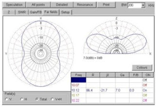
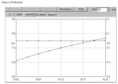
- Gain vs. Frequency Radiation pattern vs. Frequency
 If we are quite satisfied with the results of the simulation, usually we want to know the dimensions / geometry antenna. This can be done by pressing the View menu, there is cable dimensions in right side. To find out the various dimensions of the existing cable we need to use Wire Selected menu in the lower right.


December 09, 2009
Homebrew PLL for HF Band
This is a PLL design that have been tried and works well for HF bands,
based on this design can be developed more PLL for frequency other band.


1. Because this PLL works at 100 Hz step, it created the first reference frequency 100 Hz. Circuit that handles it is UNIT CLARIFIER, IC2, IC3, IC4 and IC5 is fed to the Comparator pin3. CLARIFIER produce 6144 MHz frequency changed by a digital signal IC2, IC3 divided by 4069 and divided again by 15 by IC4 thus obtained frequency 100Hz.
2. PLL design is the issue of output 5.5 MHz to 6 MHz.Output of VCO strengthened in addition to output, some output is inserted into IC1 Pin 4 to be mixed with the xtal oscillator frequency. The results of this mixing the difference is taken and converted into digital signals by the IC2 and fed to the IC19 (4059) called programmable DEVIDER.
3. In this project we design so that it is in the ON PLL's output frequency 5.7MHz. (Please design something different). The output of the mixer IC1 Pin6 is 6144 - 4440 = 5.7 Hz, which is then fed to the PROGRAMMABLE IC10 DEVIDER Pin1 for 4440 divided by the number 100 to get the results hz on pin 13. The output from IC 10 pin 13 is fed to the IC Comparator 5. Because IC5 receive 2 same frequency 100Hz then the IC 10 will be LOCK marked with LED flame. Pin output of Comparator 13 is a a constant DC voltage and fed to the varicap diode at 209 MV VCO. Thus the PLL out will also be constant or stable at 5.7MHz to Comparator LOCK, so that the output of IC5 is a DC voltage a constant and flat. This DC voltage is fed to the VCO so that the PLL stable at 5.7MHz frequency.
4. To program the IC 10 to divide the 4440, conducted via UP / DOWN consisting of counter IC6, IC7, IC8 and IC9, which each have Pin 4, 12, 13 and 3, which is used to enter the program. If PIN2 is given 9-volt voltage will have a weight like a table in the schema, while the foot that the weighted ground ZERO.
5. In this project programmed IC 6 weight 4, then 4000, weighing 7 IC 4 means 400, IC 8 weighted 4, means 40 are IC9 weighted 0, so the value of the program is = 4000 + 400 + 40 + 0 = 4440. (try it with other programs)
6. Dial Encoder with all its components to move the value of the program which is the UP / DWN counter so that the PLL to walk up / down.
Reff. Supardi yb3dd.
Amateur Radio Antenna Designing Software Use MMANA
MMANA is software to simulate antenna made by JE3HHT - Makoto Mori, DL1PBD - Alex Schewelew & DL2KQ - Igor Gontcharenko.
Using software MMANA we can calculate exactly how the size antenna should we get up for work at certain frequencies and a good match. I itself had several times to implement the results of calculations and all MMANA average obtain good results. MMANA software can be taken for free on the Internet from the address,
http://mmhamsoft.amateur-radio.ca/files/programs/MMANA-GAL-1.2.0.20.exe
Installing on a Windows PC is relatively simple, like installing other software, we just need to click on file ,

And file exe from MMANA will automatically installed on the PC that we use.
December 08, 2009
Homebrew Frequency Counter PIC16F84
This is a very useful equipment for these experiments are related to amateur radio. If we buy products so of course expensive for my pocket barely. It was lucky I found a reference from the internet about the projects of frequency counter OM3CPH radio amateurs on His site.
Once when I have not made this tool during these experiments to make the oscillator is always there constraints to find whether it is working or to know the frequency and the output is become the biggest obstacle in my hobby to make a radio projects.
Manufacturing process for circuit and I mimic the same PCB with the
which he described OM3CPH. Constituent components of this project are also many available in the market so do not be worried for him.
The result of my homebrew, fantastic until now still do well and I still use.
On the other time I would describe the experience making this frequncy counter
December 04, 2009
Text Editor for Writing Assembly Programs
Text editor is a simple word processing program used to write programs for the microcontroller. Advanced word processing course is not necessary, because it takes only ascii text-only processing.
Some programs under the Windows environment can be used such as Notepad or Wordpad (save as text document). Some of the text editor under DOS is also still usable, even more easily. The author likes Q-Edit to write programs microcontroller.
Microchip as microcontroller maker PIC16x84 provide special programs other than MPLAB which serves as a text editor as well as a compiler for the microcontroller (using MPASM) and also as progammer (for programmers such as microchips made PICSTART, PROMATE etc.)
Whatever text editor you use, one thing to remember is to give the name of the program with extension.asm. This allows us that the file is an assembler file. Basically giving the other extension also not be blamed.
Programming PIC Microcontroller with MPASM
MPASM is Microchip-made program that is used to compile the program we have created for PICmicro.After compiled microcontroller family, which has created the program will be transformed into specific codes (binary / hex) is only known by its the microcontroller .
Therefore, files generated by MPASM will with extension.hex. The following is an example of a hex file.
: 0A00000083168501831205140428FD
: 00000001FF
We do not understand the meaning of these numbers, but the microcontroller PIC16x84 will understand. After you compile your program and have made a file. Hex it is now time to put the program into the microcontroller and view performance microcontroller.
MPASM program is a compilation of the program not only for the microcontroller PIC16x84 course, but for PICmicro microcontroller families. This program is working in the Windows environment and there are unisex which DOS environment work in version 5.0 and above.
MPASM program can be used in 2 ways:
a.For produce absolute code (absolute code) that can be executed directly by the microcontroller.
b.For generate object code (object code) that can be compiled dilinked with other modules.
Source files used as input to the MPASM has a specific format. This format must be followed to prevent errors during assembly processes carried out. If there are errors in the source files, then during the assembly process will produce an error message if an error occurs, it will produce an error file (*. err) which can be read by a text editor program. Source files can be created by following the rules as follows.
Each line in the source file can contain four types of information are:
a.Label
A label must begin in the first column. This label can be followed by a colon (:), spaces, tabs, or the end of the line. Labels must begin by a letter or underscore and may contain letters, underscores or sign Tanya. Labels can use up to 32 characters in length.
b.Mnemonic
A mnemonic assembly instruction, assembler directive, calling the macro must begin in the second column or more. If there are labels on the same line, the command must be separated from that label by a colon or by one or more spaces or tabs. One or more spaces must be used to separate labels and also between the mnemonic mnemonic and Operands.
c.Operand
Operands follow the mnemonic. Operands must be separated from the mnemonic by one or more spaces or tabs. After the dot-coma by MPASM will be considered as comments and will be ignored by MPASM.
d.Comments
Comments can be included following the Operands, mnemonic or label and can begin in any column. Maximum width of the column is 255 characters.
To start using MPASM is very easy. Once you activate this program will look like in the Figure 1 will be obtained.
 Figure 1.MPASM program source input display
You can just enter the file will be compiled through the BROWSE button. After that live press the Assemble. If the source file does not contain errors, it will be shown in green as figure 3 below
 Figure 2. the result file compilation OK
 Figure 3. compilation OK report
, but if produced error will be shown in red. To find out what mistakes we have done can be seen in the *. err file that is automatically generated.
 Figure 4. the result file compilation NG
 Figure 5. compilation NG report
 Figure 6. the error message file
Note the error messages in the file *, err. Then fix the error, and compile with MPASM. If all error messages have been corrected, then the *. err file will not be produced again.
Digital decoder for PLL
In the example of the use of TTL IC this time, we will try to submit a design Switch to set UPDOWN operating frequency of a PLL which uses TC 9122. First we will take the IC 7400 to create two inputs to the flipflop as the following counter is 74192.
 Figure 1.Updown digital switch
With the above design, when the UP button is pressed, IC1 will count forward, and the calculation results will be issued as a Binary coded Decimal via pin 3, 2, 6 and 7. If the count at IC1 has reached 10, it will give one IC1 to IC2 pulses that will calculate forward IC2 and IC1 ONE count back to ZERO. BCD output is then used as input to the PLL to adjust the working frequency.
 Figure 2.Seven segment display
If the output is sampled and used as input to the IC 7447 to turn 7 segment, the results of this calculation can be displayed.
 Figure 1.Updown digital switch
 Figure 2.Seven segment display
 If the output is sampled and used as input to the IC 7447 to turn 7 segment, the results of this calculation can be displayed.
December 03, 2009
Mixer oscillator for PLL
If the crystals with the ideal frequency is not obtained, then another way to create a feedback oscillator is by mixing the two oscillators. Mixture can also be done by entering the Carrier Oscillator frequency of the plane into the mixer and mix it with 3 MHz crystal oscillator (This crystals are common in the market ). To make this mixer can be used MC1496 as Figure 1 and TA7310 the following Figure 2. If we compare between the two mixer, then a simpler circuit TA7310 and not a lot of eating places on the PCB.
 Figure 1. MC1496 mixer

Figure 2.TA7310 PLL mixer
If colleagues have advanced radio amateurs to assemble this kind of PLL along with modifications, it will easily develop with such use types other ICs. In this paper described only single-loop PLL with fellow radio amateur colleagues can continue to develop such a double-loop PLL design so obtained lengkah smaller multi-KHz and the VCO can also be developed into multiband PLL. With a little knowledge about the use of TTL ICs, the tuning frequency can be done in other ways such as with the UP / DOWN switch or can be developed again by using the Rotary decoder circuit.
 Figure 1. MC1496 mixer
Figure 2.TA7310 PLL mixer
If colleagues have advanced radio amateurs to assemble this kind of PLL along with modifications, it will easily develop with such use types other ICs. In this paper described only single-loop PLL with fellow radio amateur colleagues can continue to develop such a double-loop PLL design so obtained lengkah smaller multi-KHz and the VCO can also be developed into multiband PLL. With a little knowledge about the use of TTL ICs, the tuning frequency can be done in other ways such as with the UP / DOWN switch or can be developed again by using the Rotary decoder circuit.
Oscillator Feedback Circuit
Feedback oscillator can be assembled in other ways, for example by using MPF102 FET type, 2SK19 or 2SK192. Also on the fine tuner, can be varactor diodes are used to replace varco functions, such as the example shown in the circuit diagram of Figure below .
Similarly VCO circuit, the PCB is possible to make VCO circuit which vary. These variations are not discussed in this paper, but his fellow radio amateurs are welcome to create their own.

Similarly VCO circuit, the PCB is possible to make VCO circuit which vary. These variations are not discussed in this paper, but his fellow radio amateurs are welcome to create their own.
December 02, 2009
Component and PCB Design PLL
The type and number of components required for assembly PLL are given in Table 1 below and the layout of components on the PCB can be examined in Figure 1 and the PCB as shown in Figure 2.
List of components.
 Component parts primarily to the circuit loop filter and VCO circuit Is C1, C2, C3 and C4 is preferable to use Condensator NPO type C3, while for more preferred tantalum.
 Figure 1 Component layout PLL
 Figure 2 PCB layout PLL
How to assembly
How to install the components on the PCB is recommended to use sequential order as the following :
1. Installation of voltage regulator
2. Installation of VCO and then in a state of components in other parts not yet installed pengecheckan held output at OUTPUT terminals. The frequency of the output should be located in between 13 ~ 14 MHz.
3. Installation of feedback oscillator, then the output frequency was observed at 3 and the TEST POINT fine tuner to start, he should be able to move between the frequency of up to 12,700 + 1KHz untill 12,700 - 1KHz.
4. Installation DEVIDER 1 (TC5082) and checked on the TEST POINT 1, the output frequency must exactly 10 KHz.
5. Installation DEVIDER 2 (TC4017) and checked on the TEST POINT 2, the output frequency must exactly 1 KHz.
6. Installation of programmable DEVIDER (TC9122) and the phase detector (TC5081). With all installed components, PLL must be locked in position thumb wheel or thumb wheel 000 not installed (LED should be extinguished). If not locked, then the L1 adjusted on ferrite so that the PLL can be locked.
7. Installation of thumb wheel and then dial 999 is placed in position, the LED should remain off, if not then the ferrite from the L1 reset. In other words the PLL to the design must can be locked from the frequency to 13,700 MHz to 14,699 MHz.
8. Furthermore thumb wheel 000 is set at the position, then dial the unit level increased by equivalent to the number 9 position as observed whether the increase of output frequency exactly 1 KHz. Unless appropriate increase the frequency of 1 KHz is not swayed. So done also for the tens dial and dial hundreds. Please note that each will hold a checking, always considered first whether the component is fully installed and already well construction. Important is whether the voltage at the IC pins and pad at the foot of the transistor is correct.
List of components.
 Component parts primarily to the circuit loop filter and VCO circuit Is C1, C2, C3 and C4 is preferable to use Condensator NPO type C3, while for more preferred tantalum.
 Figure 1 Component layout PLL
 Figure 2 PCB layout PLL
How to install the components on the PCB is recommended to use sequential order as the following :
1. Installation of voltage regulator
2. Installation of VCO and then in a state of components in other parts not yet installed pengecheckan held output at OUTPUT terminals. The frequency of the output should be located in between 13 ~ 14 MHz.
3. Installation of feedback oscillator, then the output frequency was observed at 3 and the TEST POINT fine tuner to start, he should be able to move between the frequency of up to 12,700 + 1KHz untill 12,700 - 1KHz.
4. Installation DEVIDER 1 (TC5082) and checked on the TEST POINT 1, the output frequency must exactly 10 KHz.
5. Installation DEVIDER 2 (TC4017) and checked on the TEST POINT 2, the output frequency must exactly 1 KHz.
6. Installation of programmable DEVIDER (TC9122) and the phase detector (TC5081). With all installed components, PLL must be locked in position thumb wheel or thumb wheel 000 not installed (LED should be extinguished). If not locked, then the L1 adjusted on ferrite so that the PLL can be locked.
7. Installation of thumb wheel and then dial 999 is placed in position, the LED should remain off, if not then the ferrite from the L1 reset. In other words the PLL to the design must can be locked from the frequency to 13,700 MHz to 14,699 MHz.
8. Furthermore thumb wheel 000 is set at the position, then dial the unit level increased by equivalent to the number 9 position as observed whether the increase of output frequency exactly 1 KHz. Unless appropriate increase the frequency of 1 KHz is not swayed. So done also for the tens dial and dial hundreds. Please note that each will hold a checking, always considered first whether the component is fully installed and already well construction. Important is whether the voltage at the IC pins and pad at the foot of the transistor is correct.
December 01, 2009
LC Resonance Circuit VFO
High frequency and low frequency limits of this work tend VFO determined by the value of L1 and C1 (check the circuit diagram in the figure 2 above),besides of course the use of varactor. Calculation for determine the amount of L1, C1 and varactor type used seemed too complicated. However, in practice we can expect roughly taking into account L1 and C1 alone and with trial and error method we develop some results so that getting what we want. To think big about inductance L1 with a capacitance C1 we have specify, you can use the following formula calc Resonance :
 f is expressed in MHz
L is the inductance coil L1 is expressed in uH.
C is the capacitance C1 is expressed in pF.
For example in VCO design specified the desired resonant frequency 12.700MHz, while the value of 30 pF C1 is selected, then the calculation according to the formula above the value obtained L approximately 5 uH.
To make a coil with the above values should be some experiment. Based on the results of the experiment the author, when used Koker former radio IF as shown in Figure below with loops of wire Koker's former hair, then to be able to obtain the value approximately 5 uH 8T empirically necessary.
 Figure IF coil
By rotating the coil ferrite is, the value will change the inductance that can be adjusted to obtain the correct value. Please note that not all Koker have the same properties, so depending on the type of ferrite used. Experiments in above is done by using IF Koker RCL brand shop that there are many in the market,with other types of Koker will get different results.
 f is expressed in MHz
 L is the inductance coil L1 is expressed in uH.
C is the capacitance C1 is expressed in pF.
For example in VCO design specified the desired resonant frequency 12.700MHz, while the value of 30 pF C1 is selected, then the calculation according to the formula above the value obtained L approximately 5 uH.
To make a coil with the above values should be some experiment. Based on the results of the experiment the author, when used Koker former radio IF as shown in Figure below with loops of wire Koker's former hair, then to be able to obtain the value approximately 5 uH 8T empirically necessary.
 Figure IF coil
November 29, 2009
PLL Frequency Synthesizer Step 1 KHz
In principle, Phase Lock Loop is a feedback control circuit system consists of main parts as follows:
1. Phase Detector
2. Loop Filter
3. Voltage Controlled Oscillator (VCO)
Major role in the PLL phase detector is held by the duty comparing the input phase of the VCO signal with a reference signal and the output is a different phase.
The existence of different phases will provide a further voltage difference, the difference voltage is filtered by the loop filter and applied to VCO. Then the control voltage to the VCO frequency change towards minimize the difference between a reference signal with a feedback signal from VCO. If the loop becomes locked, then control voltage in a position where the average frequency of feedback signal exactly equal to the frequency reference.
The success of a PLL design is largely determined by the loop filter design good. This is because in the event of phase difference, phase detector, voltage differences will issue a change up and down. Loop filter must be able to hold sway voltage so that voltage changes into the VCO becomes smooth.
 Figure 1. PLL diagram
For the purposes of use as a regulator of the transceiver operating frequency,
various PLL can we make, but in this paper try asking a PLL design with a detailed circuit so that we can easily understand how it works. Although to fulfill that purpose is required of
many components, but with this design step can work clearly understood. In this design is used a lot of IC TC9122,TC5081, TC5082, TC4017 and TA7310.
Actually PLL circuit can be made with a fairly simple example using IC type MC145106, MC145163, and so forth there are also many on the market. These type of IC has been able to perform the function is complete, with an IC is able to perform the functions of the TC9122, TC5081, TC5082 and TC4017. But the use of IC type is not discussed in this paper.
Circuit Design
In this paper proposed a PLL design with step 1 KHz fine equipped with an analog tuner with band width of 1 to 2 KHz to allow setting more precise operating frequency (less than 1 KHz).
PLL is planned to be able to work from 13,700 to 14,699 MHz for use in transceiver with carrier oscillator or 10.7 MHz SSB filter. Working frequency is set with three-digit thumb wheel such that the number of hundreds, tens and units of KHz on the display thumb wheel can immediately show operating frequency transceiver.
If we have described, the PLL consists of several parts is generating reference frequency (1KHz), phase detector, loop filter, VCO, programmable oscillator mixing DEVIDER and feedback.
As a reference frequency generator used to charge TC5082 raised frequency of 10 KHz and the duty to share TC4017 frequency 10KHz results from TC5082 to 1KHz. 1KHz frequency is then used as comparison phase by phase detector TC5081.
For VCO in this design is used TA7310. The use of IC is intended to be at once doubled as the mixer for the purposes of feedback on the phase detector through a programmable DEVIDER. In this design the input to the programmable DEVIDER a result of the reduction of the frequency VCO with frequency crystal.
Frequency VCO and band width is set according to the needs in this design he should be able to work at a frequency of 13,700 MHz to 14,700 MHz, for used on instrument with 10.7 Mc IF. As a control frequency of the VCO varactor diodes are used. Various types of varactor can be used for example MV2205, MV2209, BA150, SMV 610 and so on. Type varactor diode of the above have a capacitance range different which can be seen in vademicum issued by the manufacturer.
Programmable devider share feedback from the VCO frequency by a factor of divider as we enter the program, the results are fed into the phase detector and compared with the reference signal. As a programmable DEVIDER TC9122 use, type of IC has the ability to share with the divisor factor until 3999.
Therefore, feedback from the VCO can not be directly input to TC9122 and must first be mixed with an oscillator frequency and the result is inputted into devider. Frekuensi mixer oscillator must be chosen so that the reduction does not exceed the ability of TC9122. For example, the PLL design is planned to work on 13,700 MHz to 14,699 MHz oscillator used mixing 12,700 MHz (the difference is 1-1999 MHz).
TC9122 programming done Binary coded Decimal (BCD) is that any decimal number represented by 4 binary digits. Entering unit numbers done by hand while the thousands (MHz) is permanently inserted directly connected pins 15 to Vdd. Entering done by thumb wheel, or can also use the Up down switch.

Figure 2. Circuit PLL
Up Down Switch for PLL
Frequency mixing crystal oscillator is selected on 12.700MHz with the intention that display numbers on the right thumb wheel with working frequency transceiver. For the purpose this often required a crystal with a frequency that is hard to find in the market. If no
crystals can be obtained with the ideal frequency as mentioned above, can also be selected crystals
with frequencies close to the consequences of viewing figures thumb wheel odds with the frequency of work.
Used as a phase detector IC TC5081 charge of comparing the phase feedback signal derived from the VCO through a programmable DEVIDER with reference signal.
The next phase detector will set the control voltage through the loop filter so that the VCO
adjust the frequency so that its phase equals with reference frequency.
In pin 4 of the TC5081 facility if there equipped with LED circuit indicator may give an indication whether the PLL in lock state or not. With the circuit as shown on the figure 2 above, the LED will light when the PLL is not locked in and will die if PLL locked.
Supply voltage electricity can be used with 5 to 9 VDC, this design used in +5 V. The use of higher supply of 5V on this design can be done without having to change the value of component values except elco and tantalum voltage that must be considered.
Reff. Sunarto YBOUSJ
November 21, 2009
My Homemade Microcontroller Programmer
This time I want to show the old version of my build own the micro-1 programmer. The tool is started I've made since I have a desire to make a frequency counter based PIC16x84. For the purposes of programming the microcontroller's I had to make this programmer. Namely the simple desire to find a series of Programmers a simple but can also be used as development board. After searching literature books and the Internet so I found a series of micro-1 was designed by our friend Ibnu malik. Below programmer I had made and successfully :


Micro-1 above I make the PCB board with holes and assemble the components in a way ugly style. It was ugly but essential function properly. Total cost : not more than $ 7 USD. That information from me hopefully inspire the reader might as well .. have fun ..


Micro-1 above I make the PCB board with holes and assemble the components in a way ugly style. It was ugly but essential function properly. Total cost : not more than $ 7 USD. That information from me hopefully inspire the reader might as well .. have fun ..
November 18, 2009
Very Useful and Cheap Development Board / Programmer Microcontroller PIC16F84
In order to load program to microcontroller PIC16F84 so we want for a circuit programmer . As usually with programmer microcontroller there will always be placed the microcontroller to socket (ZIF socket) and then load program in its.
After we load program to the microcontroller complete then release its from socket and then install into target circuit (example: robot circuit) that already prepared. However if loaded program is not working properly , so we must release microcontroller and re-load program again into programmer. And so continuous until our robot circuit working properly.
Process insert-release this chip microcontroller sure will need long time and thereby will also take time for process development our robot circuit.
For save time when process development robot circuit based microcontroller PIC16F84 so we can using a development board so-called Micro-3 computer. With using this device we unnecessary again process insert-release microcontroller.
At Micro-3 computer board there has been programmer circuit for microcontroller PIC16F84. Just only connect to computer via serial port. For programming can be done by arrange DIP switch to “PROGRAM” mode. After load program to microcontroller finished so arrange again DIP switch to “RUN” mode.
Thereby where board for programmer microcontroller and board for target circuit integrated into a board so the Micro-3 programmer have been very useful device.
For making Development board Micro-3 programmer is very easy, we only need some component that available in market such as resistor10K / 4K7 ,IC 7805, DIP switch, Socket IC and several connector.
The circuit Micro-3 programmer
 Ways of working above circuit as follow : when will going to programming to microcontroller so now connect DB9 with serial port computer. Setting DIP switch at mode “PROGRAM” on position : DIP SW1 ON, DIP SW2 OFF, DIP SW3 ON, DIP SW4 ON, DIP SW5 OFF, DIP SW6 OFF. In this case occasion microcontroller connected with circuit programmer
And after programming process have been finished then DIP switch must be turnback to “RUN” mode on position : DIP SW1 OFF, DIP SW2 ON, DIP SW3 OFF, DIP SW4 OFF, DIP SW5 ON, DIP SW6 ON. In this case occasion microcontroller isolated from circuit programmer and connected to target circuit and target circuit will working in the same manner as input program .
 3. Setting DIP switches on the micro-3 in the PROGRAM mode position.
4. Select oscillator on "XT" by clicking the radio buttons on the XT
5. Select marking on the "Power-up Timer" and others leave it blank.
Program mode
Mode is programmed microcontroller / download programs from a PC via cable
given and connect with the serial Port.
Switch 1 ON
Switch 2 OFF
Switch 3 ON
Switch 4 ON
Switch 5 OFF
Switch 6 OFF
Since the Micro-3 came in the condition not been programmed, so setting DIP switches in accordance with the Program mode. After all the above done, then the Micro-3 has been prepared to be programmed.
To ensure that the Micro-3 can be used may have been done using
following the pilot program. Write the following program in a text editor
(notepad, etc. Q Edit).
; Experiment Program for Micro-3
; File name: tesmicro.asm
;============================
processor 16f84
org 0x00
Start
movlw 0xaa
end
Save a file with a name:
tesmicro.asm
After that did compile programs using MPASM.
Find tesmicro.asm file through Browse button and then press the Assemble button will appear which indicates the process there are no mistakes.
 From this process you will get a file that is: tesmicro.hex.
After that open software programmers (picprog) and enter the tesmicro.hex file.
Do not forget to install the program voltage of +13 VDC ~ +14 VDC.
6. After that click the "Program" so that the download process will soon take place.
After a successful programming process the contents of the microcontroller PIC16F84 can be viewed using button "Read " / glasses symbol.
The results must be obtained is the value of 30AA. While other data is 3FFF. This indicates that the programmer has to function properly
 7. After the download is complete, set the DIP switches on the Micro-3 in RUN position
Switch 6 ON
8. Consider what the target circuit is working correctly. If not try to turn off the source 9 volt briefly to give Power On Reset.
9. Once we are sure that the Micro-3 works well, then now is the time you make your own program in accordance with the desired performance.
The following example is given power supply that can be used to program the Micro-3 . 
 In "Run" mode also can be used a 9 V battery.
This is because the Micro-3 has found a tool that regulate the voltage input to 5 volt voltage.
You can also use a 5 Volt voltage, but you must give to pin microcontroller that prescribed.
Arrangement of pins I / O
Micro-3 has 3 pen I / O are arranged in 2 rows. The composition of the I / O is as follows.
After we load program to the microcontroller complete then release its from socket and then install into target circuit (example: robot circuit) that already prepared. However if loaded program is not working properly , so we must release microcontroller and re-load program again into programmer. And so continuous until our robot circuit working properly.
Process insert-release this chip microcontroller sure will need long time and thereby will also take time for process development our robot circuit.
For save time when process development robot circuit based microcontroller PIC16F84 so we can using a development board so-called Micro-3 computer. With using this device we unnecessary again process insert-release microcontroller.
At Micro-3 computer board there has been programmer circuit for microcontroller PIC16F84. Just only connect to computer via serial port. For programming can be done by arrange DIP switch to “PROGRAM” mode. After load program to microcontroller finished so arrange again DIP switch to “RUN” mode.
Thereby where board for programmer microcontroller and board for target circuit integrated into a board so the Micro-3 programmer have been very useful device.
For making Development board Micro-3 programmer is very easy, we only need some component that available in market such as resistor10K / 4K7 ,IC 7805, DIP switch, Socket IC and several connector.
The circuit Micro-3 programmer
 Ways of working above circuit as follow : when will going to programming to microcontroller so now connect DB9 with serial port computer. Setting DIP switch at mode “PROGRAM” on position : DIP SW1 ON, DIP SW2 OFF, DIP SW3 ON, DIP SW4 ON, DIP SW5 OFF, DIP SW6 OFF. In this case occasion microcontroller connected with circuit programmer
And after programming process have been finished then DIP switch must be turnback to “RUN” mode on position : DIP SW1 OFF, DIP SW2 ON, DIP SW3 OFF, DIP SW4 OFF, DIP SW5 ON, DIP SW6 ON. In this case occasion microcontroller isolated from circuit programmer and connected to target circuit and target circuit will working in the same manner as input program .
How to use of Micro-3 Programmer
Micro-3 is a Development Board / Programmer to learn and use the microcontroller PIC16F84.
Using the Development Board, this will shorten the learning time and at the same PIC16F84 microcontroller can be used for real purposes.
Micro-3 is using a microcontroller-based PIC16F84 Flash memory that allows the process to erase and write 1000 times. You can program and delete much.
Therefore, the circuit based with this can be upgraded in software someday. Your
investment will remain safe. For example is you create a device-based Micro-3 , but appeared later performance demands (eg to deal with some additional sensors again) then it may be possible given the nature PIC16F84
re programmable. You can just customize the program to the performance
re programmable. You can just customize the program to the performance
demands of today.
Specification
Micro-3 has a specification as follows.
. Dimension: 9.5 cm x 5 cm
. Processor: PIC16x84
. Operating frequency: 4 MHz
. Number of I / O: 13
. Working voltage : +9 volt ~ +12 volt
. Interface : Serial (COM port)
. OS : Win 98/SE, Win 2000, Win XP
. Port available : Port A = RA0..RA4
Port B = RB0..RB7
(all port can used)
. Power supply:
a. Program: +13 VDC ~ +14 VDC
(No more !!!).
b. Run: +9 VDC ~ +12 VDC
. Relations with PC: Serial port
. Other: DIP switch regulator Run / Program

Step by Step to Use

Step by Step to Use
By the time you already made a Micro-3 , you can not directly use these tools. This is because in a state mikrokontrolernya not programmed. Therefore should be done for microcontroller programming process with the program to your liking.
The steps as follows:
1. The first open the program PICPROG (freeware) on your computer to transfer the contents of the program to Micro-3 computer. If you do not have PICPROG (freeware) you can download here.
 2. Klik icon "Open" and then select the hex extension file (*. hex) where the file is actually a compilation using MPASM or other compilers (eg MicroPascal for PIC).
 3. Setting DIP switches on the micro-3 in the PROGRAM mode position.
4. Select oscillator on "XT" by clicking the radio buttons on the XT
5. Select marking on the "Power-up Timer" and others leave it blank.
Program mode
Mode is programmed microcontroller / download programs from a PC via cable
given and connect with the serial Port.
Switch 1 ON
Switch 2 OFF
Switch 3 ON
Switch 4 ON
Switch 5 OFF
Switch 6 OFF
Since the Micro-3 came in the condition not been programmed, so setting DIP switches in accordance with the Program mode. After all the above done, then the Micro-3 has been prepared to be programmed.
To ensure that the Micro-3 can be used may have been done using
following the pilot program. Write the following program in a text editor
(notepad, etc. Q Edit).
; Experiment Program for Micro-3
; File name: tesmicro.asm
;============================
processor 16f84
org 0x00
Start
movlw 0xaa
end
Save a file with a name:
tesmicro.asm
After that did compile programs using MPASM.
Find tesmicro.asm file through Browse button and then press the Assemble button will appear which indicates the process there are no mistakes.
 From this process you will get a file that is: tesmicro.hex.
After that open software programmers (picprog) and enter the tesmicro.hex file.
Do not forget to install the program voltage of +13 VDC ~ +14 VDC.
6. After that click the "Program" so that the download process will soon take place.
After a successful programming process the contents of the microcontroller PIC16F84 can be viewed using button "Read " / glasses symbol.
The results must be obtained is the value of 30AA. While other data is 3FFF. This indicates that the programmer has to function properly
 7. After the download is complete, set the DIP switches on the Micro-3 in RUN position
Switch 1 OFF
Switch 2 ON
Switch 3 OFF
Switch 4 OFF
Switch 5 ON
Switch 2 ON
Switch 3 OFF
Switch 4 OFF
Switch 5 ON
9. Once we are sure that the Micro-3 works well, then now is the time you make your own program in accordance with the desired performance.
Power Supply
Already explained above that when the programming voltage required for +13 VDC ~ +14 VDC.

As for the mode "Run" can use the voltage +9 V ~ +12 VDC.
 In "Run" mode also can be used a 9 V battery.
This is because the Micro-3 has found a tool that regulate the voltage input to 5 volt voltage.
You can also use a 5 Volt voltage, but you must give to pin microcontroller that prescribed.
Arrangement of pins I / O
Micro-3 has 3 pen I / O are arranged in 2 rows. The composition of the I / O is as follows.
The structure is as follows:
RA1 RA0 CLK1 GND CLK2 +5 V +12 V GND Rb5 RB4
RA2 RA3 RA4 RST RB6 Ke7 RB0 RB1 RB2 RB3
RA1 RA0 CLK1 GND CLK2 +5 V +12 V GND Rb5 RB4
RA2 RA3 RA4 RST RB6 Ke7 RB0 RB1 RB2 RB3
Description:
RAx = Port A
RBx = Port B
RST = Reset
GND = Ground
Pin CLKx = Clock
+12 V = on this pen is available voltage
+12 V (+9 to +12 V or V depending on input voltage).
+5 V = on this pen is available voltage
+ 5V (regardless of input voltage).
RAx = Port A
RBx = Port B
RST = Reset
GND = Ground
Pin CLKx = Clock
+12 V = on this pen is available voltage
+12 V (+9 to +12 V or V depending on input voltage).
+5 V = on this pen is available voltage
+ 5V (regardless of input voltage).
Subscribe to:
Posts (Atom)

